By University of Warsaw, Faculty of Physics March 22, 2026
Collected at: https://scitechdaily.com/scientists-trap-light-in-a-layer-1000x-thinner-than-a-hair/
Scientists have found a way to trap light in an extremely thin layer, potentially reshaping how future photonic devices are built.
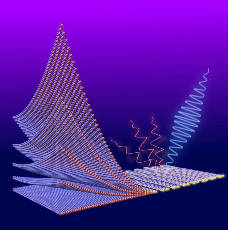
Scientists from the Faculty of Physics at the University of Warsaw, working with teams from the Łódź University of Technology, the Warsaw University of Technology, and the Polish Academy of Sciences, have created a structure that can trap infrared light within a layer just 40 nanometers thick (about 0.00004 millimeters or 0.0000016 inches). They achieved this by designing a subwavelength grating made from molybdenum diselenide (MoSe2). Their findings were published in the journal ACS Nano.
Controlling light at very small scales could transform both science and technology. As traditional electronics approach their physical limits, photonics offers a new path forward. Instead of relying on slow-moving electrons, photonic systems use fast photons to carry information. This approach could lead to devices that are both faster and smaller than current technologies.
The Challenge of Light as a Wave
Light presents a fundamental challenge because it behaves as both a particle and a wave. Every wave has a wavelength, which sets a natural size scale. For visible light, this distance is typically a few hundred nanometers. For infrared light, it can reach a micrometer or more. This raises an important question: can light be confined within structures smaller than its own wavelength?
The research team has shown that it can. They developed a structure capable of trapping infrared light within a layer only 40 nanometers thick (about 0.00004 millimeters or 0.0000016 inches). This was made possible by using a subwavelength grating built from molybdenum diselenide (MoSe2), as described in ACS Nano.
What Is a Subwavelength Grating?
A subwavelength grating is a type of diffraction grating made of closely spaced parallel strips. These structures bend and split light in a way similar to a prism. When the spacing between the strips is smaller than the wavelength of light, the grating can act like a nearly perfect mirror. At the same time, it can trap light within a very small volume.
Earlier versions of these gratings, made from materials such as silicon, gallium arsenide, or gallium nitride, needed to be several hundred nanometers thick to work effectively. If they were made thinner, they lost their ability to confine light.
To solve this problem, the researchers used a material with a much higher refractive index. In such materials, light travels more slowly. Molybdenum diselenide turned out to be especially effective. Light slows by about 1.5 times when entering glass from air and about 3.5 times in silicon or gallium arsenide, but by about 4.5 times in MoSe2. This allowed the team to shrink the grating thickness to just a few dozen nanometers, more than a thousand times thinner than a human hair.
Nonlinear Effects and Light Transformation
Molybdenum diselenide also has additional advantages. Like graphene, it is a layered material, but unlike graphene, it behaves as a semiconductor. It also exhibits nonlinear optical effects, including third harmonic generation.
In this process, three photons combine to form a single photon with three times the frequency. As a result, infrared light can be converted into blue light. This happens because three infrared photons “combine” into one, whose wavelength corresponds to the blue color. According to the study in “ACS Nano”, the strong confinement of light within the MoSe2 grating increases this effect by more than 1,500 times compared to a flat MoSe2 layer.
The study is notable not only for its performance but also for how the material was produced. Until now, thin layers of MoSe2 were typically created by exfoliation, the same method used for graphene. This involves peeling layers from a crystal using adhesive tape.
Although simple, exfoliation is not very reliable and produces only small samples. The typical size is around ten square micrometers, which is too small for most practical applications, including photonic integrated circuits.
To overcome this limitation, the researchers used molecular beam epitaxy (MBE), a standard method for producing semiconductor layers. This technique had not previously been applied to materials like MoSe2.
A Breakthrough in Fabrication Methods
The results were significant. The team produced uniform MoSe2 layers covering several square inches, all with a consistent thickness of 40 nanometers (about 0.00004 millimeters or 0.0000016 inches). This creates an extreme aspect ratio of about one to a million. For comparison, a typical sheet of A4 paper has a ratio of about 1:2000.
These findings suggest that molybdenum diselenide produced in this way could change how scientists control light. Thick structures are no longer required. Instead, ultrathin layers just a few dozen nanometers thick can achieve strong light confinement and enhanced optical effects. Because the production method is scalable, the technology could move beyond the lab and into real-world applications.
Reference: “Optical Bound States in the Continuum in Subwavelength Gratings Made of an Epitaxial van der Waals Material” by Emilia Pruszyńska-Karbownik, Tomasz Fąs, Katarzyna Brańko, Dmitriy Yavorskiy, Bartłomiej Stonio, Rafał Bożek, Piotr Karbownik, Jerzy Wróbel, Tomasz Czyszanowski, Tomasz Stefaniuk, Wojciech Pacuski and Jan Suffczyński, 26 February 2026, ACS Nano.
DOI: 10.1021/acsnano.5c12870
The research was funded by the National Science Centre under projects OPUS 2020/39/B/ST7/03502 and 2021/41/B/ST3/04183, with European Union funds under ERC-ADVANCED grant No. 101053716, the Foundation for Polish Science under project ENG.02.01-IP.05-T004/23, and by the University of Warsaw under the Excellence Initiative – Research University (IDUB) New Ideas in Priority Research Areas II No. 501-D111-20-2004310 titled “Ultrathin subwavelength gratings based on dichalcogenides.”
Leave a Reply