February 11, 2026 by Pohang University of Science and Technology
Collected at: https://techxplore.com/news/2026-02-ai-analog-layout.html
Researchers at Pohang University of Science and Technology (POSTECH) have developed an artificial intelligence approach that addresses a key bottleneck in analog semiconductor layout design, a process that has traditionally depended heavily on engineers’ experience. The work was recently published in the journal IEEE Transactions on Circuits and Systems I: Regular Papers.
Semiconductors are used in a wide range of technologies, including smartphones, vehicles, and AI servers. However, analog layout design remains difficult to automate because designers must manually arrange structures that determine performance and reliability while meeting a large number of design rules.
Automation has been especially challenging in analog design because layouts are too complex and design strategies differ significantly by circuit. In addition, training data is scarce, since layout data is typically treated as proprietary and is rarely shared outside companies.
The POSTECH team, led by Professor Byungsub Kim in the Department of Electrical Engineering, focused on the “foundation model” approach. A foundation model is first pre-trained on large-scale data and can then be adapted to different downstream tasks with relatively little additional training. The researchers applied this concept to analog layout design.
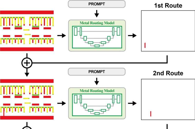
The key method is self-supervised learning, in which the model learns without human-provided labels. The team divided analog layouts into small patches, masked part of each layout, and trained the model to predict the missing layout elements. Using this procedure, the researchers generated about 320,000 training samples from six real layout datasets.
After pre-training, the model learned repeated structures and patterns commonly found in analog layouts. With limited additional data, it was then adapted to five layout-related tasks: contact generation, via generation, dummy pattern insertion, N-well generation, and metal routing. In experiments, 96.6% of the generated layouts reportedly passed both design-rule checking and layout versus schematic verification. The team also reported that comparable performance was achieved using one-eighth of the data required by conventional approaches.
The study suggests that a single foundation model can be leveraged for multiple analog layout tasks, reducing the need to build a separate model for each task. The researchers said the approach could reduce design workload and shorten development time, improving productivity in semiconductor design.
“This work meaningfully expands the practical feasibility of automating analog semiconductor layout design, which has been constrained by data scarcity,” Professor Kim said. First author Sungyu Jeong said, “The main contribution of this work is the methodology that enables large-scale learning.” He added, “Our goal is to collect more data and continue developing the foundation model to a practically usable level.”
The study was conducted by Professor Kim, Ph.D. candidate Sungyu Jeong, Wonjun Choi, and Junwoong Choi, and master’s graduate Anik Biswas (currently at Samsung Electronics).
More information: Sungyu Jeong et al, A Self-Supervised Learning of a Foundation Model for Analog Layout Design Automation, IEEE Transactions on Circuits and Systems I: Regular Papers (2026). DOI: 10.1109/tcsi.2025.3615646
Leave a Reply