February 25, 2026 by JooHyeon Heo, Ulsan National Institute of Science and Technology
Collected at: https://techxplore.com/news/2026-02-reveals-power-noiseless-clock-circuit.html
A research team affiliated with UNIST has announced the successful development of a novel semiconductor circuit capable of generating high-quality clock signals with significantly reduced noise levels. This innovation combines a compact design with low power consumption, addressing critical challenges in high-speed communication and computing technologies.
Clock signals are fundamental to the operation of modern semiconductor chips, synchronizing billions of tiny devices to ensure seamless data processing. As the demand for faster data rates in 5G, 6G, artificial intelligence (AI), and high-speed interconnects continues to grow, the quality and stability of these signals become increasingly vital. Noise components like reference spurs, which can impair system performance, have posed persistent challenges in high-frequency clock generation.
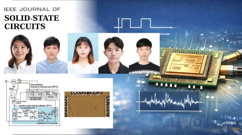
Led by Professor Heein Yoon from the Department of Electrical Engineering, the team has developed an injection-locked clock multiplier (ILCM) circuit that significantly minimizes reference spur noise. While traditional ILCM designs are effective in reducing jitter—the rapid timing fluctuations—they often generate residual noise called “reference spur,” which can limit overall system accuracy. The study is published in the IEEE Journal of Solid-State Circuits.
Utilizing a simplified design based on a ring voltage-controlled oscillator (VCO), the team’s circuit demonstrates remarkable performance at a frequency of 2.1 GHz, achieving a record-low reference spur level of -81.36 dBc—the lowest reported worldwide for ring VCO-based ILCMs. Additionally, it delivers an ultra-low jitter of only 280.9 fs, suitable for ultra-high-speed applications.
Fabricated using 28nm CMOS technology, the circuit occupies just 0.0444 mm² and consumes only 12.28 mW of power. Its compact size and energy efficiency make it ideal for space-constrained and battery-powered devices, including mobile phones, IoT sensors, and next-generation communication modules.
A key aspect of this innovation is its ability to suppress reference spur noise without increasing circuit complexity or power consumption. The researchers achieved this by integrating a frequency tracking loop and a timing calibration method that dynamically optimized the injection timing, effectively minimizing residual noise sources that lead to reference spur.
Professor Yoon explained, “Injection locking offers a fast and efficient way to generate high-frequency clock signals, but the residual reference spur has always limited system performance. Our design reduces this noise with a simple, yet highly effective, circuit structure—opening new avenues for high-speed, low-power semiconductor systems.”
Publication details
Hyeonjun Nam et al, A Low-Reference-Spur Injection-Locked Clock Multiplier Using Sub-Sampling Frequency Tracking Loop and Injection Pulse Timing Calibrator, IEEE Journal of Solid-State Circuits (2026). DOI: 10.1109/jssc.2025.3650135
Journal information: IEEE Journal of Solid-State Circuits
Leave a Reply