February 23, 2026 by Sungkyunkwan University
Collected at: https://techxplore.com/news/2026-02-generation-ai-semiconductors-thermal-constraining.html
A research team led by Professor Taesung Kim from the School of Mechanical Engineering at Sungkyunkwan University has developed a technology that precisely controls the internal structure of semiconductors using heat, much like stamping out “bungeoppang” (fish-shaped pastry) in a mold. The team report that this approach improves the performance of next-generation artificial intelligence (AI) hardware. With this technology, complex AI computations can be processed more quickly using significantly less electricity than before. The findings are published in the journal ACS Nano.
From von Neumann to in‑memory
Most computers and smartphones we use today operate based on the “von Neumann architecture.” This structure is similar to having a desk (the processor) and a bookshelf (the memory) placed far apart.
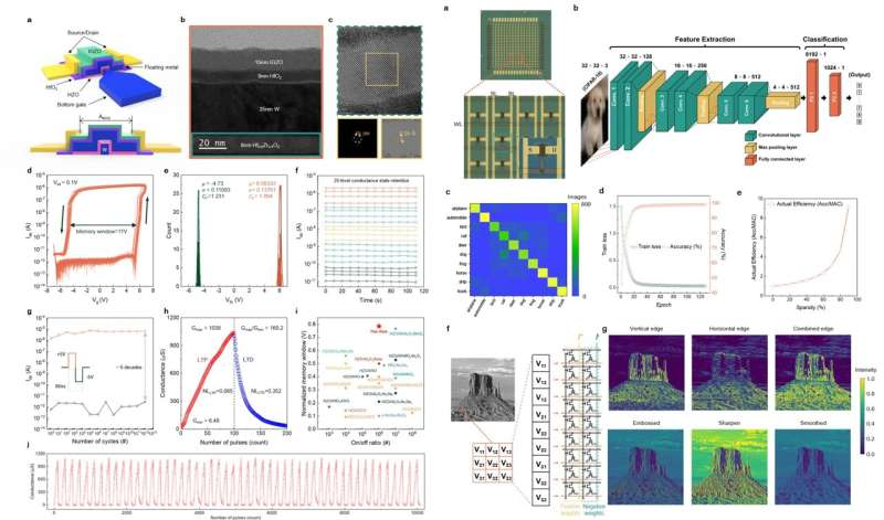
Each time you study, you have to go back and forth to get a book, which takes time and effort. To solve this problem, a method called “in-memory computing” has been proposed, in which computation is carried out directly inside the memory. The key component that enables this approach is the “ferroelectric transistor,” which is the focus of this study.
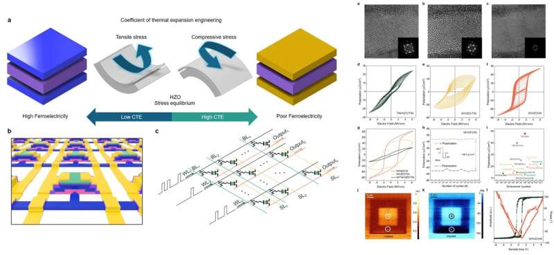
Conceptual Illustration of a Hafnium–Zirconium Oxide Ferroelectric Transistor Array Using Tungsten Electrodes and Its Implementation in Artificial Intelligence Hardware. Credit: Sungkyunkwan University
Challenges with hafnium oxide control
However, hafnium oxide, the material used to fabricate this device, is very difficult to handle. For the memory function to operate properly, the internal atoms must be aligned in a specific crystal structure (orthorhombic phase). When the material is made very thin, this atomic alignment is easily disturbed, leading to reduced performance.
In previous approaches, other chemical elements were mixed in to address this issue, but such methods involved complicated processes and had limitations in large-scale production.
Harnessing thermal expansion forces
Professor Kim’s research team introduced the physical principle of “thermal expansion.” Different materials expand and contract by different amounts when exposed to heat.
The team designed the electrode surrounding the semiconductor material so that, as it cools and slightly contracts, it applies a compressive force to the hafnium oxide inside. Like tight-fitting clothes shaping the body, this physical force generated by heat aligns the atoms into the crystal structure most suitable for memory operation.
Semiconductor devices fabricated using this new method were very thin and remained stable even after operating more than one trillion times. In addition, when these devices were connected and used for image recognition tasks in an artificial intelligence system, they achieved an accuracy of 97.2%.
This result shows that high-performance AI semiconductor devices can be realized through temperature control without relying on complex chemical processes.
Professor Taesung Kim explained, “The key point of this research is that we overcame the limitations of next-generation semiconductors through physical design based on thermal force, rather than chemical modification. If this technology is commercialized, AI could operate more intelligently and efficiently in devices where power consumption is important, such as autonomous vehicles and smartphones.”
Publication details
Geonwook Kim et al, Thermal Expansion-Engineered Ferroelectric Transistor Arrays for Scalable Edge AI Computing, ACS Nano (2026). DOI: 10.1021/acsnano.5c14095
Journal information: ACS Nano
Leave a Reply