
December 1, 2025 by Caitlin Ryan, Scientific Writer and Imogen Pass, Scientific Content Collaborator, Ossila Ltd.
Collected at: https://www.eeworldonline.com/can-chiplets-save-the-semiconductor-supply-chain/
We’re making more semiconductors than ever before, and yet somehow, it’s still not enough. Demand is continuously increasing, spurred by the rise of AI in our everyday lives, but production still faces bottlenecks. The problem is more than just scale; it comes down to the structure of the manufacturing industry as a whole. As of now, the semiconductor industry is highly centralized and dependent on just a handful of fabs. Beyond this, there’s increasingly complex geopolitics involved, with everyone wanting to be the hub for developing these advanced chips. Still, only a few countries have the infrastructure, expertise, and raw materials to make it happen.
Enter chiplets, modular, mix-and-match building blocks, which have been ranked in the MIT Tech Review’s 10 breakthrough technologies of 2024. These offer a different path through the manufacturing process, where instead of fabricating monolithic processors in a single facility, you can assemble systems from smaller, specialized dies. It is said that this approach could ease pressure on supply chains and provide us with a new level of design flexibility. But is that realistic, or just wishful thinking?
What are chiplets?
The semiconductor industry has a problem: the ongoing demand for us to keep building more powerful (and often more complex) processors is growing slowly and is very vulnerable to supply chain hiccups. That’s where chiplets come in. These are small, modular chips designed to focus on one task and do it very well. For example, a single chiplet might be a processor core, a memory block, or a graphics unit.
On their own, chiplets are just building blocks that can’t achieve much. But once they’re combined with a standard interface, you can create a fully customized system-on-chip (SoC) tailored to precisely what you need. Importantly, it is possible to eliminate unnecessary components from traditional “one-size-fits-all” chips. That means faster development and more efficient chips, overall.
We’re already seeing chiplet-based architectures from the giants of the semiconductor industry. AMD’s EPYC processors have demonstrated their scalability, and Intel’s Meteor Lake was the first of Intel’s mobile processors to use a chiplet architecture. Apple is also in on this with its M1 Ultra architecture, which reportedly has over 110 billion transistors and showcases high-performance integration for creative workloads in particular.
How could chiplets help?
At a glance, chiplets look like the solution engineers have been looking for. The chiplet-based design enables the creation of SoCs from smaller, function-specific dies. These individual modules can be optimized independently for performance and power efficiency and then integrated via a standardized interconnect. Even putting them close enough together makes it possible to cut latency and reduce energy lag in those interconnects.
The real advantages emerge when we examine how the supply chain differs between chiplets and standard monolithic SoCs. Unlike monolithic chips, chiplets don’t need to be built all at once and in the same place. A CPU core could come from one foundry, an AI accelerator from another, and an I/O block from another country entirely. This is a direct challenge to the industry’s current reliance on a few highly centralized fabs.
Chiplets that have been designed, tested, and validated can be reused across multiple products, thereby shortening design cycles and improving overall return on investment. The smaller dies required to fabricate the chiplets are also an advantage, as they result in a higher yield per wafer. Scrap rates are reduced because defects occur only in individual tiles rather than entire monolithic chips.
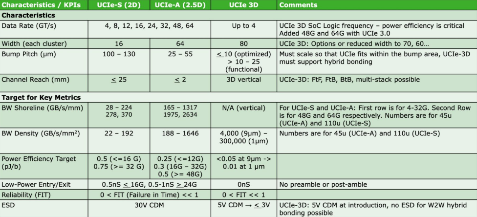
Work is underway to ensure industry-wide standardization, with standards such as the Universal Chiplet Interconnect Express (UCIe) enabling chiplets from multiple vendors to integrate with one another. Set up by chip industry leaders in 2022, hardware vendors have only recently begun releasing technology based on UCIe specifications, with IP offerings from Synopsys and Cadence kick-starting the effort. IP offerings are essential to the successful adoption of UCIe standards because, for most companies, producing UCIe-compliant chiplet designs from scratch is prohibitively difficult and expensive. This approach has the potential to decouple SoC production from the rigid supply chains we’re currently used to, providing us with greater flexibility and resilience against fluctuating demand and manufacturing constraints. But right now, UCIe is likely overkill for mid-range designs and is only moving towards becoming a mandatory standard for large data center, AI, and networking SoCs.
The not-so-small problems with chiplets
Despite their promise, chiplets still come with some very real challenges that can’t yet be ignored. Starting with packaging, the advanced process of assembling multiple dies into a single, functional unit. Aligning these tiny chiplets with extreme precision so that performance is maintained across the entire package is far from easy. Technologies like 2.5D and 3D integration are quickly improving, but they add further cost and complexity that the industry is still learning how to manage. Just as in other areas of semiconductor manufacturing that rely on a controlled working environment, these packaging steps require exceptional precision and protection against contamination.
And while chiplets can, in theory, be manufactured in different places and stitched together, in practice, much of the world still depends on expertise concentrated in the semiconductor powerhouses of South Korea and Taiwan. This means that the supply chain is vulnerable, even if the production of individual chiplets becomes more geographically diverse.
Then there’s the still-present performance issues. Chiplet SoCs suffer from increased latency and reduced power efficiency due to the connections between chiplets, with the exact impact varying by architecture, chiplet size, and packaging technology. Issues like latency and skew don’t just affect processing speed but can also influence thermal behavior and long-term reliability. Integrating multiple dies requires advanced co-design between hardware and packaging teams, and, even then, the result may fall short of the seamless efficiency achievable with a single, monolithic chip.
To counter these performance issues, testing needs to be planned across at least three levels: at the individual die level, between dies, and at the system level. As with all testing, the goal is to identify defects early. In multi-die assembly, multi-level testing using precision tools is needed to ensure only good parts are assembled, minimizing costly failures. On top of this, fault tolerance is also required at multiple levels because chiplet SoCs introduce new failure modes. These include spare lanes within chiplets to prevent a broken, weak, or noisy lane from killing the entire system or even extra chiplets in case of whole chiplet failure; error-checking codes when data moves between chiplets handle temporary problems that corrupt data; and chiplet health monitoring and isolation tracks degradation and isolates faulty chips to prevent wider failure. Coordinating these testing and fault-tolerance requirements across different suppliers could prove difficult and lead to greater inefficiencies than expected in the quality assurance of multi-die systems.
Beyond this, there are potential issues surrounding intellectual property that could arise. In a mixed-vendor SoC, who really owns the IP for that? Would the largest companies in the semiconductor industry really be willing to adopt a decentralized model if it meant sharing IP and margins? Standards like the UCIe are a good start, but the field is still relatively new and widespread adoption will take some time.
What work is being done now?
Making chiplets a more mainstream solution will take more than engineering; change needs to come from the ecosystem as a whole. Intel is already pushing in that direction through its Intel Foundry Services, which aims to support an accurate multi-vendor chiplet model. We’re also starting to see significant investment in advanced packaging fabs to handle the delicate, high-density integration that these devices require.
The widespread adoption of chiplets could transform commercial industries such as automotive and IoT. In the automotive industry, the rising demand for autonomous and advanced driving features is stretching the capabilities of conventional chips. Chiplets are a promising solution for next-gen software-defined vehicles. In late 2024, imec launched the ACP, which encourages pooling resources and expertise from across the automotive value chain to more effectively tackle key technical challenges and identify optimal chiplet architectures for high-performance automotive computing.
Some of the most significant investments are coming from the defense and aerospace industries, which are banking on chiplets to deliver the performance specs they require. However, the developments pushed these industries to look different from commercial chiplet requirements. Priorities lie in creating secure chiplet ecosystems to prevent supply-chain tampering and guarantee the authenticity of every chiplet within a system. At the same time, their packaging development focuses on accommodating combinations and SoC designs that commercial markets do not require. But solving these complex challenges could make it easier for commercial markets to implement innovative packaging and testing technologies.
Another important aspect is EDA (electronic design automation). Designing a chiplet-based SoC means managing massive levels of complexity. Think about multiple dies from different sources and processing nodes, and the need to manage performance integrity across the whole package. EDA tools can automate the analysis and simulation of chip/package interactions at different stages of the design process, identify errors such as thermal and mechanical failures, enable pre-silicon validation of the die-to-die interconnect, and more. In other words, they simplify an incredibly complex process, enabling multi-die designs while allowing them to be tested quickly before committing to expensive hardware and manufacturing processes.
EDA tools are actively being developed and improved, with options available from Siemens, MZ Technologies, and Keysight that address the design and manufacturing challenges of 2.5D or 3D ICs, technologies that directly underpin chiplet integration. Yet these tools are practically inaccessible to mainstream engineers in smaller startups, as they require specialist knowledge to use effectively. Since standards like UCIe benefit greatly from EDA tool support, as UCIe reaches broad maturity by 2030, EDA tools should become increasingly accessible. In return, effective UCIe implementation will provide a more detailed framework for simpler automation in the tools themselves.
Summary
Chiplets won’t solve every problem in the semiconductor supply chain, but they might help to ease some of the biggest ones. Moving beyond traditional single-node monolithic designs could allow us to distribute production more broadly and reduce some of the risks tied to centralized manufacturing.
Still, though, achieving this will depend on more than just clever design. To make chiplets actually work at scale, the industry needs better packaging systems and stronger standards for interconnects. Finally, more robust frameworks need to be put in place to address concerns surrounding intellectual property.
Leave a Reply