November 25, 2025 by Hanyang University
Collected at: https://techxplore.com/news/2025-11-frontend-gbs-pam.html
High-voltage, higher-order PAM-8 signals are essential to achieve data rates beyond 100 Gb/s, requiring highly linear receivers to maintain excellent signal-to-noise ratios.
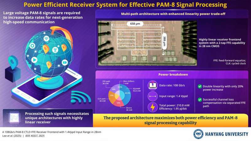
In recent work, a team of researchers, led by Mr. Sangwan Lee, an integrated M.S. and Ph.D. degree student in electronic engineering, and Dr. Jaeduk Han, an Associate Professor of electronic engineering at Hanyang University, South Korea, has proposed a multi-path architecture with an enhanced linearity-power trade-off.
The novel highly linear receiver frontend system with two-tap feed-forward equalizer (FFE) capability in 28nm CMOS exhibits a remarkable data rate of 108 Gb/s and an input range of 1.4 Vppd with 210.8 mW total power and 1.95 pJ/bit efficiency.
This next-generation technology was presented at the IEEE Asian Solid-State Circuits Conference (A-SSCC).
Mr. Lee said, “In this research, we have maximized both power efficiency and signal processing capability through two unique architectures for processing ‘PAM-8’ signals, which are essential for next-generation high-speed communication.”
The researchers first dramatically improved the linearity-power trade-off through a “multi-path architecture.” They designed the architecture by dividing the signal path, allowing each path to handle a sub-range of the total dynamic range.
As a result, the number of required slicers or samplers was reduced, decreasing the load on the final stage and facilitating the achievement of remarkable efficiency: doubling the linearity with only a 20% power increase.
Next, the team effectively compensated for channel loss through a “separated FFE path.” Since high-speed signals suffer significant channel loss, compensation via an FFE is essential. However, in conventional receiver architectures, the FFE must directly process large-voltage signals, leading to signal compression.
The researchers designed a structure that completely separates the FFE path from the main path, allowing it to calculate the compensation value using only a small, attenuated signal. This approach fundamentally prevents compression, enabling successful channel loss compensation even while handling large input signals.
This technology is poised for immediate application as a core component in next-generation high-speed data communication infrastructure.
Its key application areas include data centers and artificial intelligence (AI) clusters, wherein dramatically increasing the communication speed between servers can significantly facilitate the training of large-scale AI models and the processing of massive datasets, as well as next-generation networking equipment that forms the foundational technology for future 800G and 1.6T Ethernet systems.
Furthermore, the present research could help accelerate the computational speed of supercomputers used in advanced scientific research and simulations.
In the next five to 10 years, this work will serve as the foundational technology that accelerates the development of next-generation applications, including more powerful and widespread AI, metaverse and AR/VR era, and sustainable data centers.
“It will provide the backbone for complex AI services like real-time translation, advanced medical diagnostics, and autonomous driving systems to become faster and more universally available. Moreover, by providing the massive bandwidth required for immersive virtual and augmented reality experiences, it will help make a seamless virtual world a reality. Lastly, as global data demand continues to explode, our power-efficient approach will help reduce the energy footprint of data centers, contributing to sustainable technological growth,” concludes Dr. Han.
More information: A 108Gb/s PAM-8 CTLE+FFE Receiver Frontend with 1.4Vppd Input Range in 28nm

Leave a Reply